The basis for the manufacture of optoelectronic components are inorganic or organic carrier materials – so-called substrates – in the form of printed circuit boards made of silicon, ceramics or organic polymer materials. In order to produce conductor paths on these carrier materials, the conventional approach is to metallize the substrate on the entire surface. By means of photolithographic processes and masking techniques as well as subsequent chemical etching techniques, this metallization is then partially removed and thereby structured.
In PhoenixD, no material will be removed in order to achieve the required target structure – instead, additive manufacturing processes are developed in order to produce novel photoelectronic components flexibly and in a resource-saving manner. The researchers at the IW have set themselves the task of contributing to this with new material concepts and partial metallization processes for the carrier materials.
Metallization by additive solder coating
Non-metallic materials such as glass and ceramics can be metallized by applying active brazing alloys to the surface by vacuum heat treatment. In order to be able to additively manufacture conductor paths on non-metallic substrates, the researchers at the IW are developing a process in which the active braze metal is deposited evenly in the form of a fine powder on the surface of ceramic and glass-like carrier materials. A laser beam then melts the braze powder locally at the points where the conductor path is to be created. After the laser treatment, the non-melted part of the braze powder is removed and the conductor path metallization remains. The excess braze powder is collected and can be re-used for the next metallization.
In order to create the narrowest possible, geometrically defined conductor paths, the braze powder must be as fine as possible and applied very evenly to the substrate. Another challenge is the exact focusing and dosing of the laser energy required to melt the powder locally. The objective is to achieve conductor paths with a maximum width of 0.1 mm and a height of only 0.05 mm.
Substrates made of metal-polymer composites
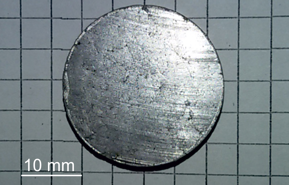
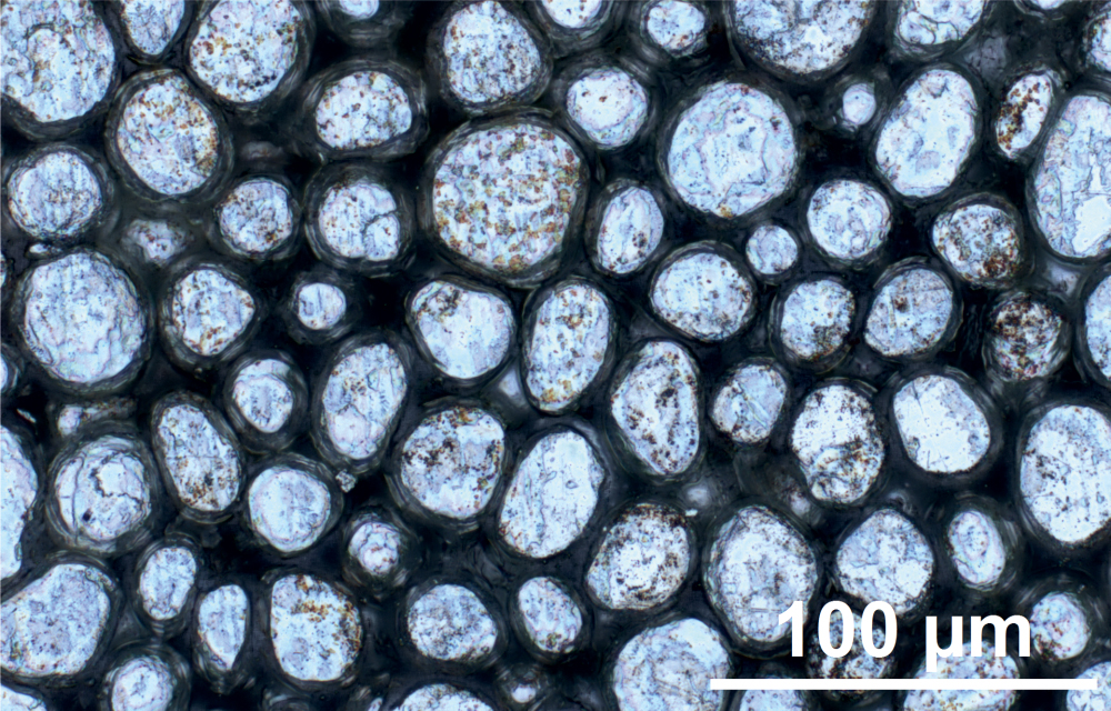
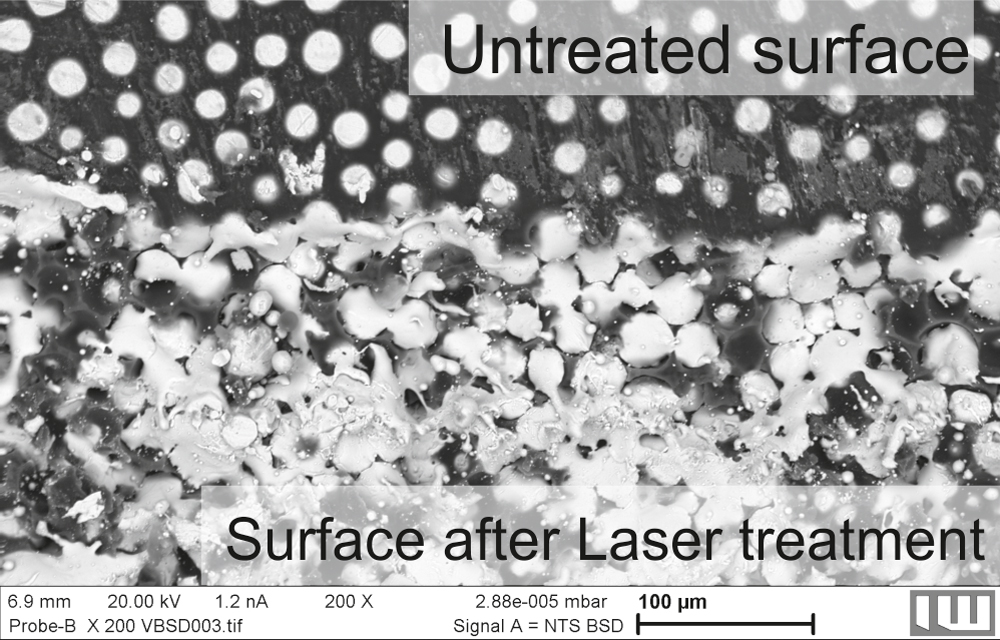
In addition, the IW working group is pursuing an approach for a carrier material that is new from both a physical and production engineering point of view. Specifically, metal-polymer composites will be used, which are made from thermoplastics and powdered metal fillers – for example, copper, aluminium or tin. With this approach, metallic volume fractions of up to 70 percent can be achieved. Provided the metal powders are suitably pre-treated, the composite material remains electrically insulating, but at the same time exhibits high thermal conductivity and temperature resistance.
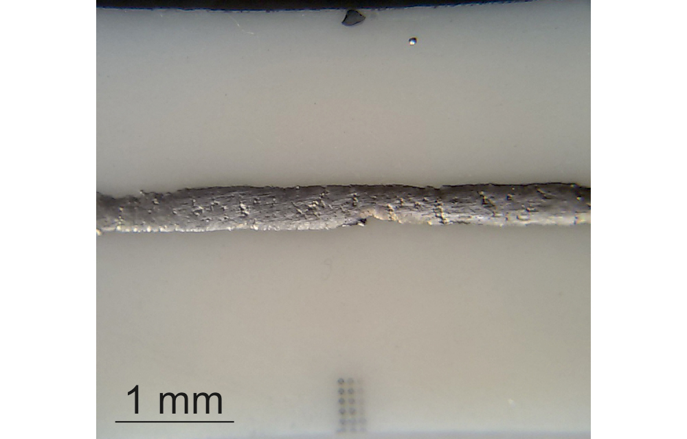
Initial tests have shown that fine conductive structures can be written into the surface of these composites by laser treatment. This is because both polymer and metal are locally liquefied by the laser beam. The metal particles fuse along the laser track to form a continuous conductor path, thereby displacing the polymer. The IW scientists now want to investigate in more detail the process variables that finally control the quality of the conductor paths. They are investigating the production of the conductor tracks as a function of the selected composite materials, the external process conditions and the laser processing parameters used.
The objective is to identify suitable composite materials and process parameters with which conductor path structures can be produced in small dimensions and high quality that are suitable for optoelectronic applications.