Skip to content
  • Newsletter
  • About us
  • Contact
  • EN
  • DE
  • Newsletter
  • About us
  • Contact
  • EN
  • DE
Search
Close
  • Overview
  • Research
  • Here & now
  • Smart minds
Menu
  • Overview
  • Research
  • Here & now
  • Smart minds
  • Overview
  • Research
  • Here & now
  • Smart minds
  • Contact
  • Newsletter
  • About us
Menu
  • Overview
  • Research
  • Here & now
  • Smart minds
  • Contact
  • Newsletter
  • About us
Search
  • EN
  • DE
1. December 2015

Slimming down sensors

IMPT | Thinner, more accurate and more versatile – these are the demands on future sensors. IMPT scientists work on a technology to deposit sensors without any intermediate layers directly on components of arbitrary size.

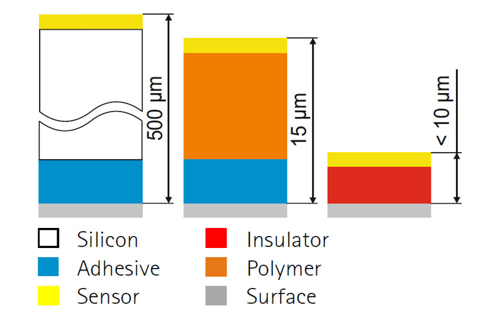
Sensors detect the air-mass flow in combustion engines, deformations in machine tools and humidity in the passenger compartment. Micro sensors are generally manufactured on carrier substrates and glued to the measuring point. The disadvantage: Thick carrier substrates and the ageing of glue may cause incorrect measurements.
Within the scope of the Collaborative Research Centre 653, a novel approach managing without the aforementioned intermediate layers is investigated at the Institute of Micro Production Technology (IMPT). Sensors are directly deposited on technical surfaces reducing measurement errors and the thickness of sensors (see Figure 2).
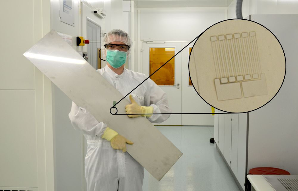
To coat components of arbitrary size with sensors, the IMPT has invented and patented a mobile coating system. A prototype was constructed in cooperation with an industry partner. In the past, components had to be inserted into the vacuum chamber of a coating system. In future, the chamber is simply put on the component, i.e. the surface of the component is the chamber’s one side. In this way, the system can directly be used in an industrial production line.

by Daniel Klaas

At a glance

  • New manufacturing technology for sensors by direct deposition
  • No carrier substrate or glue required
  • Novel approach allows for thinner sensors with higher measuring accuracy
  • Unthinkable sensor positions possible
  • Patented manufacturing system: coating of components without size limitation
IMPT_SFB-653_Bild1_01
Figure 1: Thumbs up! Daniel Klaas presents a test structure successfully deposited on a component. (Photo: IMPT)
IMPT_SFB-653_Bild2_EN
Figure 2: Distance between sensor and component gets smaller and smaller (from left): Silicon-, polymer-based and directly deposited sensors. (Graphic: IMPT)
IMPT_SFB-653_Bild3_01
Figure 3: View into vacuum chamber of patented system during coating process. (Photo: Daniel Klaas)
Previous
Next

Contact

Dipl.-Ing. Daniel Klaas

+49 (0) 511 762-18028

klaas@impt.uni-hannover.de

http://www.sfb653.uni-hannover.de/en-us/Pages/Teilprojekt-S1.aspx

This Page

drucken

recommend

  • tweet 

This Page

drucken

recommend

  • tweet 

ISSN 2198-1922 | Legal Information | Privacy notice | Article Sitemap