A novel production process for the generation of 3D conductive tracks on spatial circuit carriers is being developed at ITA within the research project "3D-CopperPrint". The circuit carriers are wetted with copper-filled pastes and the tracks are then treated in a subsequent laser sintering process.
In contrast to conventional MID technology, no chemical metal deposition is used which is extremely harmful to the environment. In addition, less process steps are needed and the process is not limited to specific substrate materials.
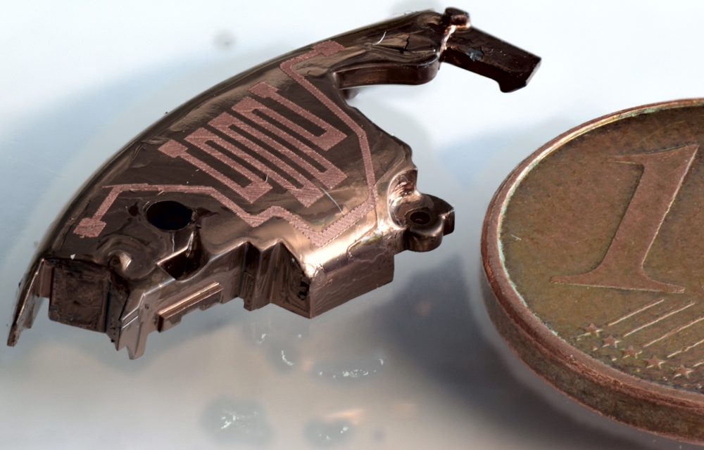
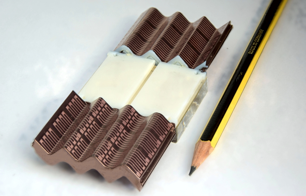
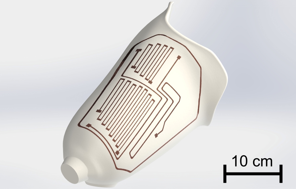
The innovative process is a progressive development of additive manufacturing. Using 3D printing, electrical functional elements can be created directly on the component surface (see Figure 2). This bears high potential in batch production. Thinkable are medical applications like tailored hearing aids (see Figure 1) or hip implants with electronic functions (see Figure 3).


