60 years ago, computers filled entire rooms; today they fit in your pocket. Scientists in the Cluster of Excellence PhoenixD now want to herald this enormous technological leap, which electronic systems have undergone, for optical systems as well.
From table to stamp format
Precision optics in micro format, mass-produced at low cost – that is the goal of PhoenixD. Unlike electronic systems, optical systems do not consist of conductor paths, resistors and transistors, but of mirrors, filters, optical switches, diodes, lenses and much more.
Usually, optical systems are built in quantity 1 on a large surface – in table-tennis format, so to speak. PhoenixD is researching miniaturisation to bring thousands of such systems together on small surfaces – in stamp format, so to speak.
An extraordinary assembly process
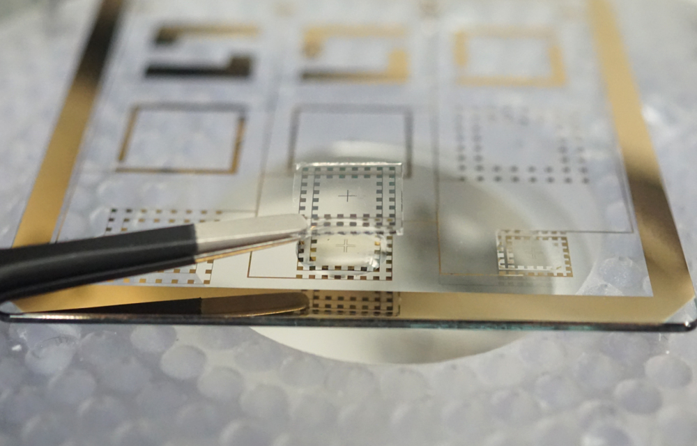
In order to manufacture cost-effective optical microsystems, the components must be precisely positioned and aligned with each other as well as layered on top of each other. The scientists at the Institute of Assembly Technology (match) pursue an innovative approach to solving this problem: they use self-assembly techniques.
This involves precisely aligning the components by using physical effects and forces. Self-assembly is carried out completely without actuators, robots or grippers, which are necessary in conventional automated assembly. Assembly takes place without handling, without active positioning by humans or machines.
As part of PhoenixD, the match is working with other institutes to research and develop designs and systems to position and align two planes exactly with each other.
Self-assembly: fast, precise and error-resistant
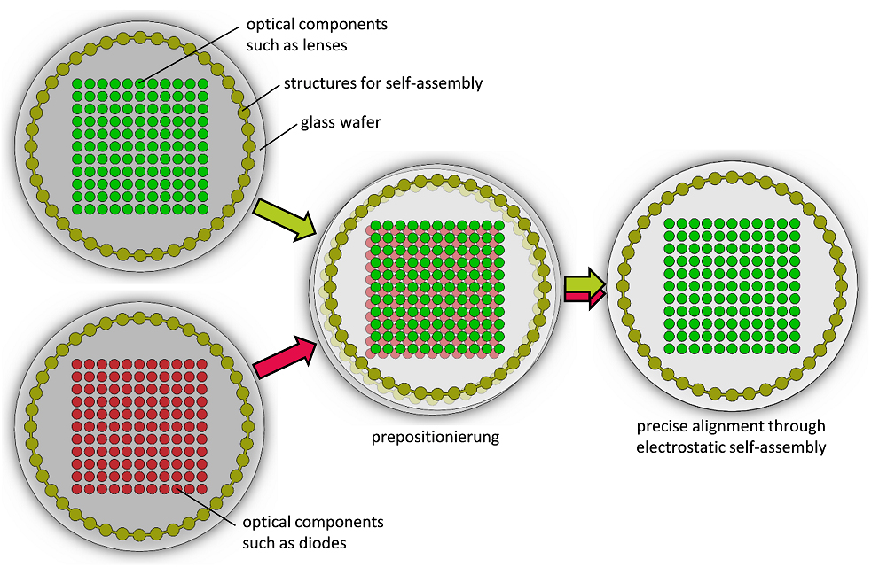
Figure 3 shows an application example on a 4-inch wafer. This wafer is equipped with 11×11 lenses. A second wafer is equipped with 11×11 diodes at exactly the same positions. Both wafers are identically coated with voltage conducting structures. These identical structures ensure that the components are positioned exactly and precisely to each other.
To do this, the two wafers must first be roughly aligned one above the other. There may be UV adhesive between the wafers, for example. This is initially liquid and forms a sliding film. When a voltage is applied, electrostatic fields and forces are generated which, in the case of initial incorrect positioning, are so great that the system attempts to adopt a state of least incorrect positioning. After rapid alignment, the UV adhesive cures, fixing the two wafers together.
This process is fast, precise and error resistant. Man and robot need considerably longer for the same work steps and are only similarly precise in exceptional cases.
In order to use self-assembly techniques, specially adapted designs are required, as well as identical structuring and exact pre-processing of the components onto the wafers.


