Skip to content
  • Newsletter
  • About us
  • Contact
  • DE
  • EN
  • Newsletter
  • About us
  • Contact
  • DE
  • EN
  • Overview
  • Research
  • Here & now
  • Smart minds
  • Overview
  • Research
  • Here & now
  • Smart minds
  • Overview
  • Research
  • Here & now
  • Smart minds
  • Contact
  • Newsletter
  • About us
  • Overview
  • Research
  • Here & now
  • Smart minds
  • Contact
  • Newsletter
  • About us
Search
  • DE
  • EN
29. January 2019

Ultra-fast assembly by consistent kinematics

ITA | To enable the production of larger quantities of smaller chips, ITA is investigating an ultra-fast assembly technology for electronic components. The researchers are using laser technology for the contactless transfer of bare chips onto a substrate.

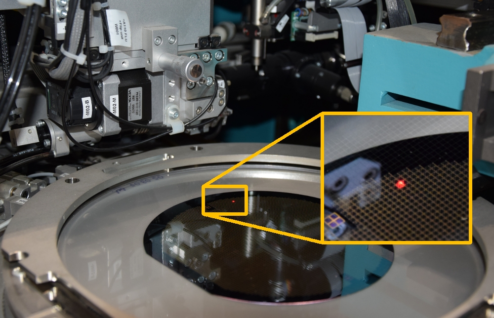
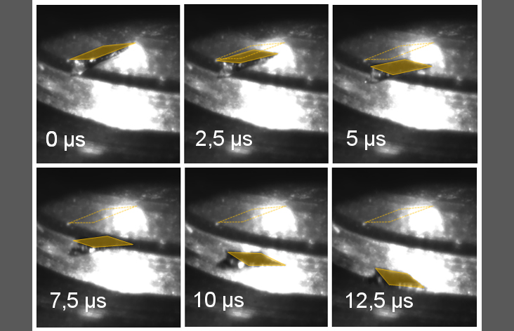
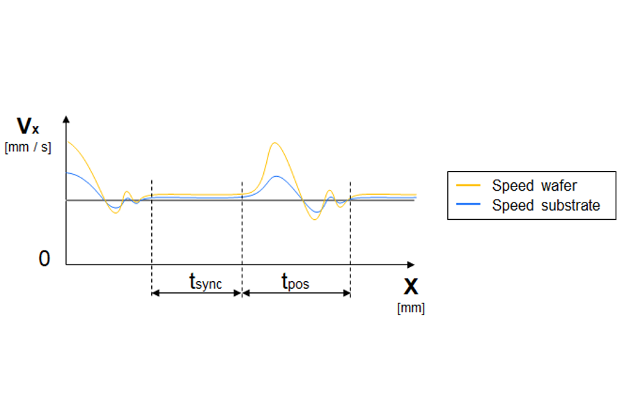
In electronics industry, there is a constant demand for ever-smaller chips – combined with increasing production numbers. The challenge: the handling of small-sized components and the assembly and bonding of more components on substrates in less time. State-of-the-art mechanical assembly technologies with an assembly rate of 20,000 components per hour for components with an edge length of 150 micrometres are pushing their technical limits. The newly developed assembly technology is based on laser technology for the contactless transfer of components. The researchers are now relying on a continuous movement of wafer, containing the electronic components, and substrate to increase the assembly rate. The aim of the research consortium is to realize an assembly of electronic components with an edge length of 30 to 150 micrometres, a positioning accuracy of plus/minus ten micrometres and an assembly rate of up to 100,000 components per hour.

by Simon N. Gottwald

Similar posts

  • Printing and forming of optical waveguides

At a glance

  • Innovative assembly technology for electronic components
  • Laser-based process transferring wafer onto substrate
  • Increased assembly rate by consistent movement
ITA_Ultraschnelle-Bestueckung_Bild1_01
Laser-based transfer of electronic components. (Source: Simon N. Gottwald/ITA)
ITA_Ultraschnelle-Bestueckung_Bild3_01
By removing the adhesion of the glue the silicium fragments are seperated from the wafer. (Source: Daniel Albrecht/LZH)
ITA_Ultraschnelle-Bestueckung_Bild2en
Split movement profile: consistent kinematics increases assembly rates. (Source: Simon N. Gottwald/ITA)

Contact

Simon N. Gottwald M.Sc.

(+49 511) 762 - 18159
simon.gottwald@ita.uni-hannover.de
www.ita.uni-hannover.de

This Page

drucken

recommend

  • tweet 

Similar posts

  • Printing and forming of optical waveguides

This Page

drucken

recommend

  • tweet 

ISSN 2198-1922 | Legal Information | Privacy notice | Article Sitemap