Sensors based on piezoelectric materials are utilized in many ways in today’s microsystems technology with the direct piezoelectric effect as the sensor’s working principle. When a force acts on the surface of the material, the resulting deformation generates a measurable charge. Depending on the polarization of the piezoelectric material, either forces acting perpendicular to the surface (normal forces) or forces acting in parallel (shear forces) can be measured. How much charge is generated depends on the piezoelectric material and can be expressed by the so-called piezoelectric charge constant. One material that has a particularly high charge constant is the ceramic lead zirconate titanate (PZT). As a result, even small forces generate a sufficiently large measurement signal.
The manufacturing process
In order to resolve forces locally and thus to be able to determine whether the forces vary depending on their location, the IMPT works on the development of a new type of force sensor array. The array consists of a group of sensors of the same type and is manufactured on the basis of the dice-and-fill method. For this purpose, 35 µm wide kerfs are first cut in an orthogonal, grid-like array in the PZT using a precision dicing process. However, the 500 µm thick PZT is only structured to a depth of 300 µm and the kerfs are filled with epoxy resin afterwards. Mechanically processing the ceramic, despite the fact that it is very sensitive due to its brittleness, could only be achieved through time-consuming studies to determine the optimum process parameters.
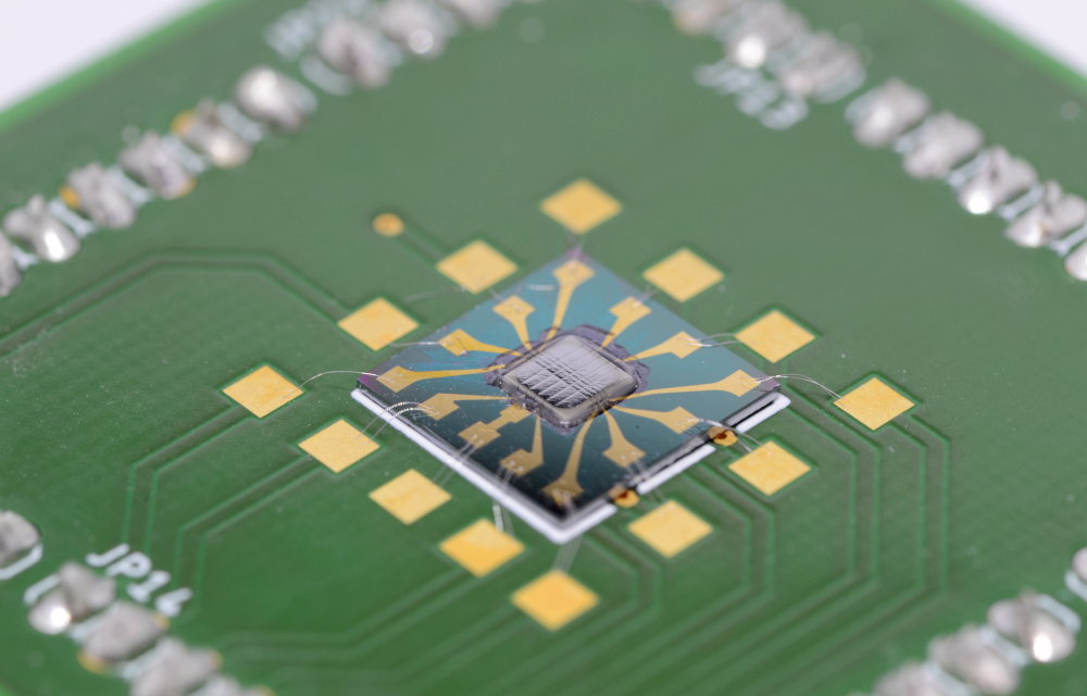
After the epoxy resin has cured, redundant filling material on the surface and the still connected ceramic at the bottom are removed in a combination of grinding and polishing processes. The result is a sensor chip with twelve sensor columns made of PZT, each measuring 365 µm x 165 µm x 300 µm, connected only by the epoxy resin filler. The filling material has the task of reducing the mechanical coupling and the resulting interference between the individual sensors. Investigations have shown that the epoxy resin can reduce the coupling to the directly adjacent sensor column from almost 100 % to around 20 %.
Afterwards, each sensor column is electrically connected individually along a microtechnological process chain that involves high-precision bonding of the sensor chip to a larger contacting chip and a printed circuit board (see photo).
Future application
The sensors are currently being used in a project funded by the German Research Foundation (DFG) to investigate the ultrasonic wire bonding process. In this case, force measurements help to investigate local effects at the wire-substrate interface and the formation of the wire bond over the course of the process time. The information obtained should help to overcome existing process limitations so that higher yields, improved bond qualities or shorter process times will be possible in the future.
Since the sensors can be easily adapted, future applications are countless and can be found wherever forces are to be measured with spatial resolution in the smallest of spaces. Due to the enormous potential, further optimization of the sensor array is being pursued in current research. In this context, reducing the area of each sensor would for example result in an even higher spatial resolution.
