The piezoelectric effect has many applications in today’s microsystems technology. Piezoelectric materials can be used to realize sensors and actuators. A distinction is made between the direct and indirect piezoelectric effect. With the direct piezoelectric effect, a voltage can be tapped when a force acts on the material – possible areas of application include pressure sensors and energy harvesting. In the indirect piezoelectric effect, a voltage is applied that leads to a deformation of the material, such as in oscillating crystals.
Aluminum nitride (AlN) is one of the commonly used piezoelectric materials in thin-film technology. For example, it offers less risk of contamination than lead zirconate titanate and can be used at higher working temperatures than zinc oxide. In its wurtzite structure, AlN exhibits piezoelectric properties. This hexagonal arrangement can be deposited as a thin-film on a substrate via various processes – for example, physical or chemical vapor deposition.
The coating process
The Institute of Micro Production Technology (IMPT) has been able to establish a coating process for AlN using reactive cathode sputtering at the institute’s own facilities. In this process, atoms are knocked out of an aluminum target in a vacuum by means of plasma. With the addition of nitrogen, the atoms are deposited in the process chamber as aluminum nitride on the substrate to be coated. By varying the process time, thin-films in the nanometer and micrometer range can be produced.
There are several ways to structure these films. First, during the process, the areas that are not to be coated can be covered with a shadow mask. The IMPT can produce such masks in-house, for example with submillimeter cutters that can be used to apply any structures in the micrometer range. On the other hand, it was possible to implement wet chemical structuring in an alkaline environment. This allows the structuring to be adapted to the process conditions.
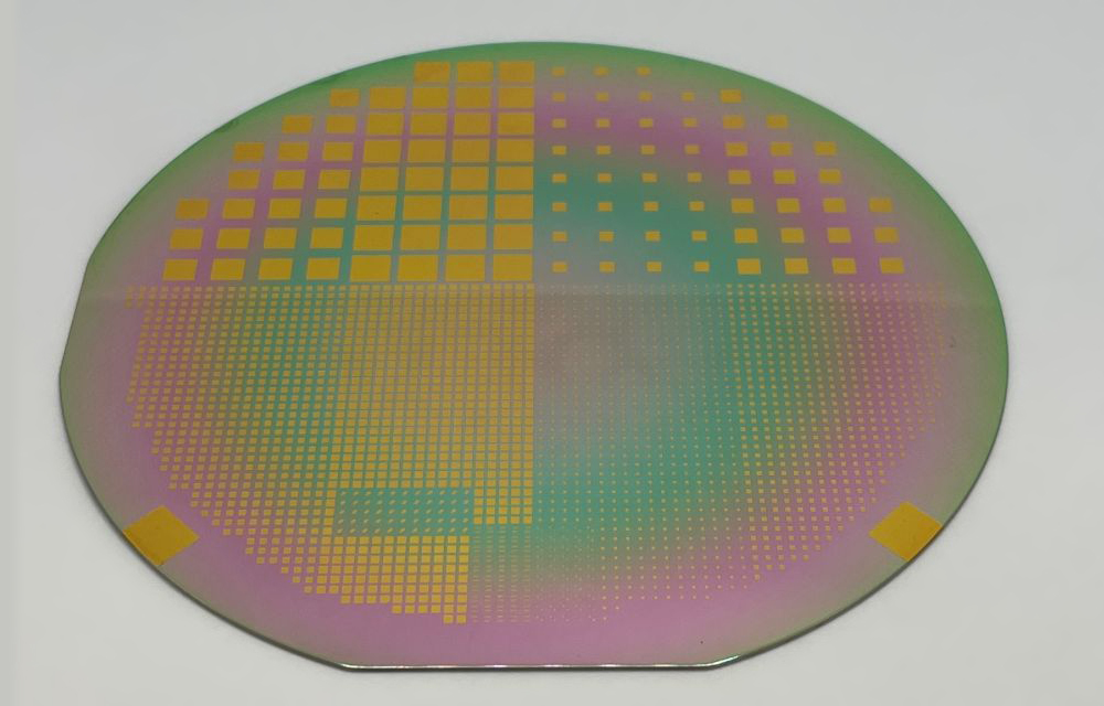
The existing possibilities for depositing electrically conductive layers also enable the IMPT to extend the process and apply electrodes that serve to contact the AlN layer. In just a few process steps, simple piezoelectric systems can thus be realized at wafer level. Internally, the deposition takes place on 4-inch substrates, so that several systems can be produced on one wafer in one process run, whereby the process itself offers the possibility of scaling.
The properties of the thin-film
Characterization of the deposited films showed that the crystal structure of the deposited aluminum nitride has a c-axis orientation, which already suggests possible piezoelectric properties of the thin-film. This was subsequently confirmed at IMPT using laser Doppler vibrometry.
In a two-electrode contact, the AlN layer could be excited by applying a voltage, thus inducing a deformation of the piezoelectric layer. Using lasers, deflections of several picometers could be measured due to the optical interferences and similar piezoelectric coefficients could be detected as known from current literature. A high dielectric strength of up to 1.42 MV/cm was also demonstrated.
The quality of the coating was also tested using in-house electroplating. The test was intended to detect possible porosity of the deposited thin-film, which could lead to a short circuit of the drive electrodes in a complete system. Analysis in the existing scanning electron microscope with energy dispersive X-ray spectroscopy showed that only very isolated to no pores were present in the film.
Future application
IMPT is only at the beginning with aluminum nitride coating. So far, the focus has been on establishing a functioning coating process and characterizing the produced layer. This showed that a functioning piezoelectric layer is available, which is now to be used by the institute in sensor and actuator systems.
Possible applications here would be pressure sensors, acceleration sensors or actuators for precise deflection. Another conceivable application would be in the field of energy harvesting for energy conversion by the piezoelectric element and thus for supplying energy to other components in the system.