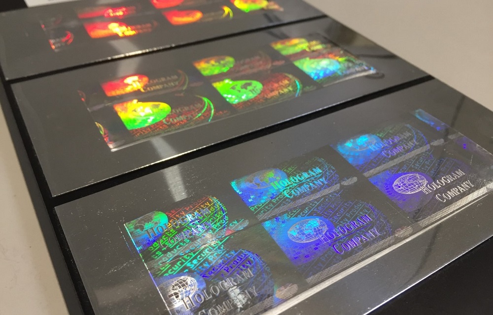
Scientists at the Institute of Forming Technology and Machines (IFUM) are investigating and analyzing a variety of forming processes – including the embossing process, in which the surface of a workpiece is modified under high pressure. Embossing as a manufacturing process for structured functional surfaces enables a high output rate at low cost per component. The competences at IFUM range from the design of individual embossing tools to the embossing of diffractive microstructures, such as rainbow holograms in metal.
Precise positioning of embossing dies and transfer of smallest structures
The embossing of micro- and especially nanostructures places particularly high demands on the machines and tools used and the precision with which the forming is carried out. Machine and tool-related disturbance variables are often unavoidable – these include guide inaccuracies, bearing play or temperature-related expansions in the drive train. But also the operational wear of various machine and tool elements has a significant influence on the embossing result. In addition, the material-specific effects must also be taken into account when designing the embossing process.
All these effects can be counteracted with active process control. Within the framework of the Cluster of Excellence PhoenixD, scientists at IFUM are developing a technical solution that makes it possible to compensate for external influences on the embossing process. With the help of innovative drive engineering and new types of measuring technology, they want to ensure the exact positioning of the embossing die so that micro and nanostructures can be transferred reproducibly with a particularly high quality.
This novel production method makes it possible to emboss diffractive structures in the nanometer range, for example in plastic foils. These are to be used in future in optical precision systems. Even the smallest deviations from the nominal geometry considerably impair the subsequent function.
Possible application: Production of optical waveguides
Two areas of application are currently emerging within the framework of PhoenixD, in which the embossing of micro- and nanostructures represents a promising manufacturing process for low-cost components in precision optics.
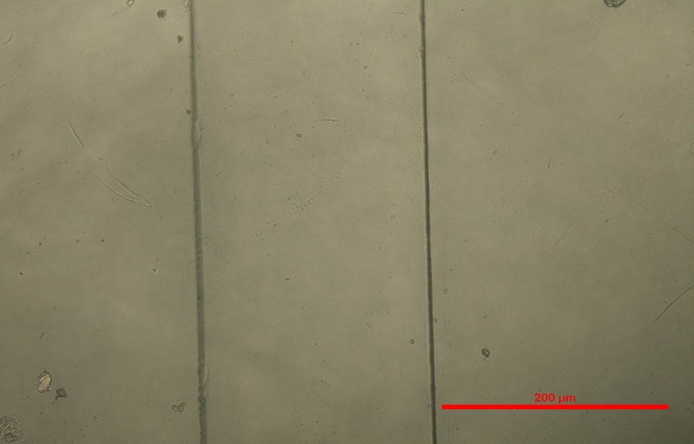
One area of application is the manufacture of single-mode optical waveguides. In this process, large-area, channel-like structures are embossed in plastic foils, which are then further processed at the Institute of Transport and Automation Technology (ITA) using the flexographic printing process. The required structures are produced at the Institute of Micro Production Technology (IMPT) by means of galvanic moulding and fixed on the embossing die.
Another field of application is the insertion of a diffractive structure on an already existing optical fibre. In this way, for example, a so-called coupling grating can be created, which makes it possible to couple the light into or out of the optical fibre.
First embossing tests at the IFUM provide promising results regarding the achievable accuracies.