When developing charging technologies for electric cars, the focus is on two main challenges: charging capacity and charging speed. More than 30 partners from six European countries are working on the aspect of charging speed as part of the EU project “Gallium Nitride for Advanced Power Application” (GaN4AP).
The main aim is to minimize the time difference between electric charging and conventional refueling with fossil fuels. To explain how the research project aims to achieve this improvement, the basics of charging electronics are important.
Basics and research overview of charging electronics for electric cars
Transforming voltages in the smallest possible space requires high frequencies. The voltage from the socket has a low frequency of 50 Hz, which requires relatively large transformers and corresponding power supply units. Nevertheless, the charging power supply units for cell phones or laptops, for example, have become smaller and smaller over the years or can transmit ever higher charging currents and voltages with the same dimensions. This has been achieved by using higher frequencies than the mains frequency (50 Hz).
To generate the higher frequencies, the AC voltage from the socket is first converted into DC voltage and then converted back into AC voltage with a higher frequency such as 1 kHz via a switch and various filter electronics (transformation in the frequency range). The switch reverses the poles of the DC voltage with the switching frequency, resulting in an AC voltage.
Mechanical switching at frequencies above 1 kHz is not feasible for the mass market, so electrical components known as metal-oxide-semiconductor field-effect transistors (MOSFETs) are used for switching. The transistors are built on silicon. These are the same components that are also used as the basis for processors.
Gallium nitride MOSFETs to increase the charging speed
MOSFETs have three connections, which allows them to act as switches. The presence or absence of a voltage at the gate terminal determines whether or not a current can flow from the source terminal to the drain terminal. In order to increase the charging speed, the parameters of MOSFETs on silicon have been pushed further and further. However, research in the field of charging technology for electric cars has now reached the limits of silicon. Alternative substrate materials are therefore being researched, such as gallium nitride (GaN).
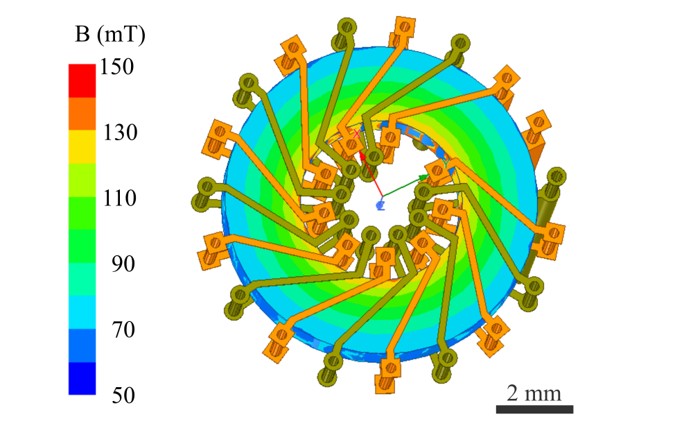
Gallium nitride has a higher electron mobility and a higher insulation barrier and can operate at higher frequencies. The increased electron mobility reduces the circuit resistance so that losses during charging are minimized. The higher insulation barrier allows the use of higher voltages at charging stations, which enables an increased charging capacity with the same charging current. The higher frequency in turn enables a reduction in the size of the components on the board, including the inductive elements.
Saving space with planar inductive components
Inductive components consist of a coil that is usually wound around a ferromagnetic core. A current flow through the coil generates a magnetic field, which can be amplified by the permeability factor of an inserted core.
Inductors are one of the three basic passive components, along with resistors and capacitors, and are required for a variety of circuits. By using several coils on one core, coupled systems can be set up to enable transmission, galvanic isolation and also transformation of alternating voltages. In a MOSFETs, for example, a transformer is used as galvanic isolation for control purposes.
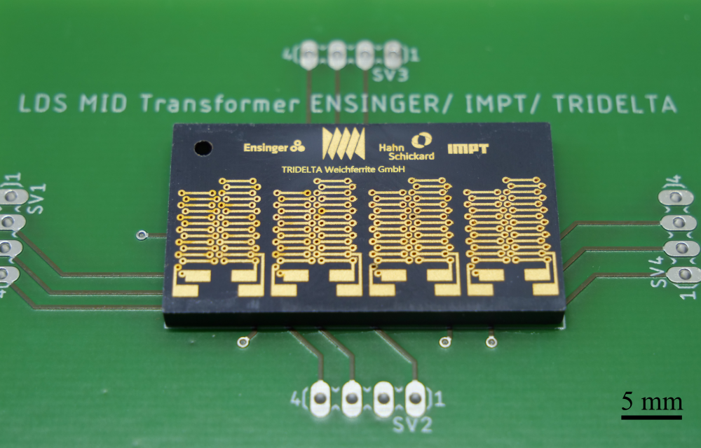
As part of the research project, the IMPT is developing planar, space-saving inductive components. These components have a maximum height of 5 mm, which opens up new application possibilities. The inductive components can either be used as substrate carriers or attached to the circuit board as individual parts and electrically connected, similar to a component. In the latter variant, the planar design also saves space, which can be taken up by larger elements such as cooling elements.
Although planar, inductive components can already be produced by researchers using PCB technology, high production costs and the lack of a mass production process pose a challenge. The space savings achieved have so far been disproportionate to the increased costs.
Plastic-based transformers and inductors
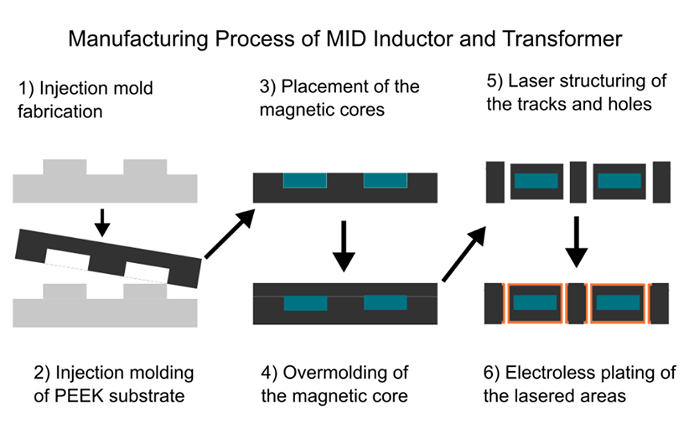
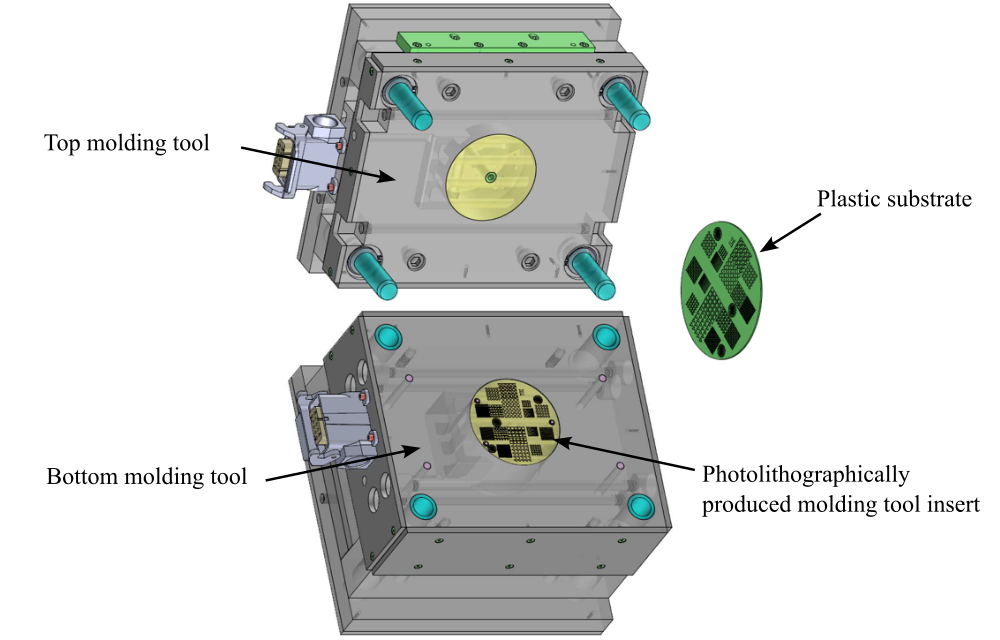
In order to enable more cost-effective production for the mass market, the IMPT is developing an innovative manufacturing process that is not based on printed circuit boards, but instead uses injection molding and the plastic polyether ether ketone (Tecacomp PEEK LDS black, Ensinger GmbH). This approach produces so-called molded interconnect devices (MIDs), or MID inductors and transformers.
The MID inductors and transformers are produced in a two-stage injection molding process. In the first stage of injection molding, the substrate is created into which the core material MnZn ferrite is inserted. MnZn ferrites are one of the few materials that still exhibit high permeability values even at high frequencies of one megahertz. In the second stage of injection molding, the core is completely encapsulated with PEEK. In addition, additives in the PEEK enable the surface to be activated by laser. The activated surface enables selective deposition of copper, which is used to produce the coils around the core. After this process, the inductors and transformers can be characterized and integrated into demonstrators.
Advantages of MID inductors and transformers
The MID inductors and transformers have several advantages over conventional inductors and transformers in SMD design. The typical winding of inductors, even more so for transformers, requires highly complex and costly winding machines. In the MID process, these machines are completely replaced by a laser system and electroless deposition.
The use of the laser system also makes it easy to adapt the coil design. Interwound coils, which offer improved transmission properties for transformer systems, can be produced more easily. As the MID components already have a plastic housing, further processes for housing production are no longer necessary.
Cooperation with Ensinger for the production of MID transformers
Due to the promising results, the IMPT has developed a constant industrial cooperation with Ensinger GmbH. The company contributes its expertise in injection molding and encapsulates the ferrite cores using two-stage injection molding. The IMPT is responsible for the design, layout, characterization and, in part, for the laser structuring and deposition of copper.
Together with Ensinger, the IMPT is driving forward the industrial production of MID transformers and supporting the transition to electromobility.