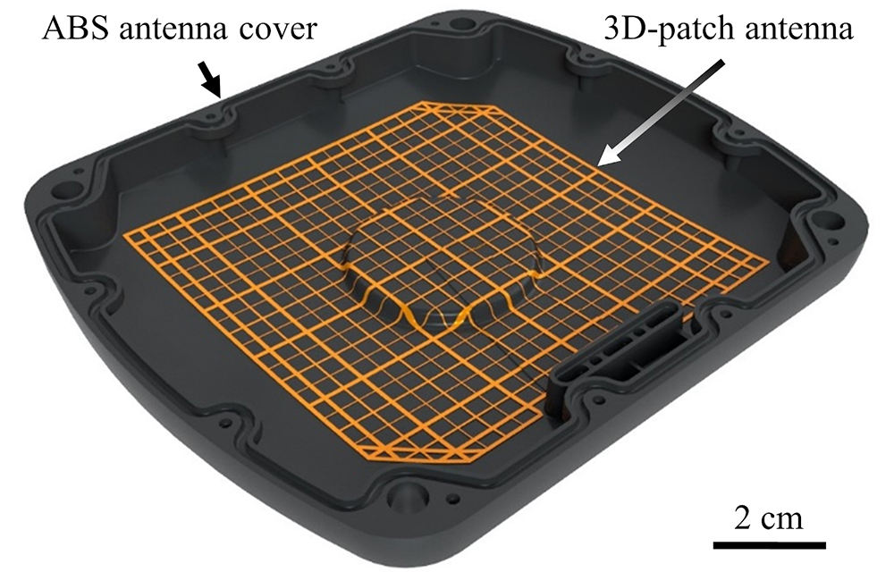
During the research project 3D-CopperPrint at the Institute of Transport and Automation Technology (ITA), Ejvind Olsen successfully printed a conductive copper grid on a three-dimensional surface.
3D printing of conductive traces
The process consists of several sub-steps. First, a primer is applied to compensate for surface defects and ensure adequate thermal insulation of the component. Then a copper-containing ink is applied, which is sintered by a laser to form conductive copper traces. In the final step of the process, laser cleaning is used to remove the remaining non-sintered ink. The procedure thus represents an innovative way to produce hybrid electrical-mechanical components.
Award-winning conference paper
Olsen presented his research findings at the 14th International Congress MID, which took place from 8 to 11 February 2021, as an online conference. He received a Best Paper Award for his associated paper, “Printing of laser-generated conductive copper traces on 3D components,” which included prize money of 500 euros.
In the award-winning paper, Olsen illustrates the process applied to a three-dimensional antenna cover (see Fig. 2). For more information on the 3D-CopperPrint project, visit https://www.ita.uni-hannover.de/en/institute/team/m-sc-ejvind-olsen/research-projects/projects/3d-copperprint/.
Information about the conference can be found at https://www.3d-mid.de/en/congress-mid/ and https://www.3d-mid.de/en/the-first-virtual-mid-congress-was-a-great-success/.