Due to an increasing number of electronic devices in every area of life, the electromagnetic fields used for communication are also increasing. These can overlap and lead to signal interference with each other, especially at high data rates.
Optical data transmission is not affected by these interferences – because photons are not electrically charged. Over long distances, the use of optical fibers as optical waveguides is already established in this respect. For short distances, however, there is still no cost-effective solution since the production and the planar integration of large quantities of optical waveguides in printed circuit board systems have so far presented complex production challenges.
Research objective: Flexible optical printed circuit board
To get to the bottom of this problem, the Institute of Transport and Automation Technology (ITA) is conducting research along the entire process chain together with industrial partners in the BMBF joint project OptiK-Net (direct printing and integration of optical short-haul networks).
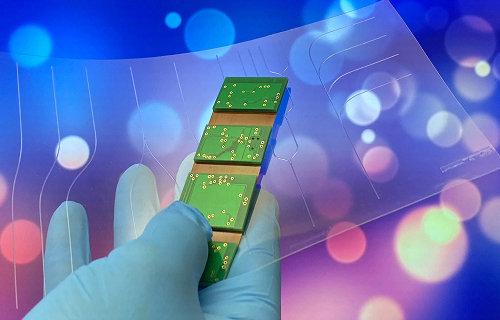
The aim is to produce an optical flex printed circuit board (see Fig. 1). The fundamental questions here are how polymer optical waveguides – adapted to PCB integration – can be produced by printing and how integration into conventional PCBs can be implemented industrially.
Printing optical waveguides in a variety of ways
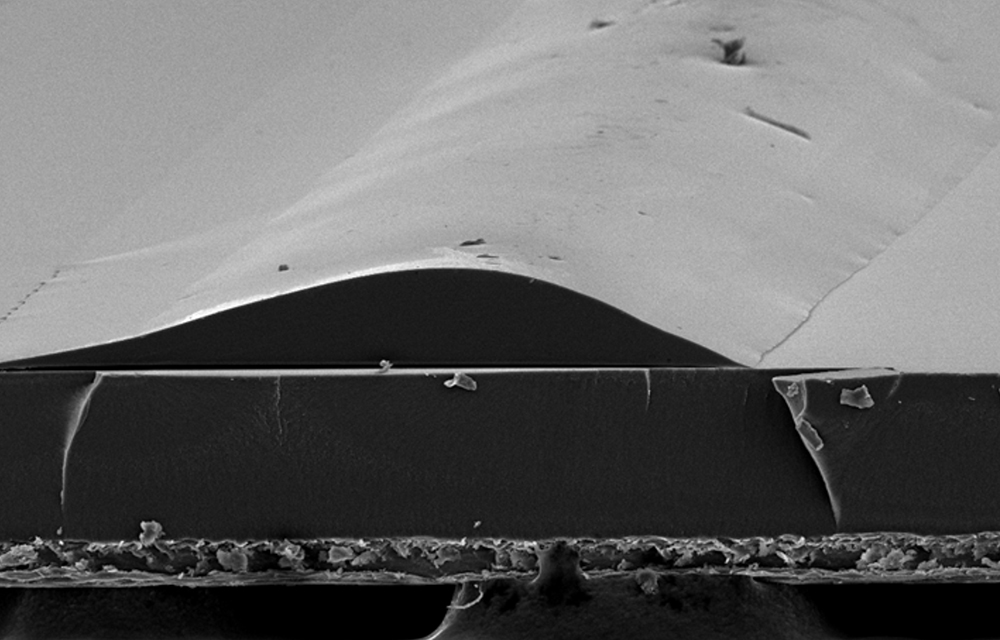
The research association is investigating gravure printing (Janoschka), screen printing (Gallus) and flexographic printing (ITA) as manufacturing processes for the optical waveguides. The aim is to produce optical waveguides using each of these printing processes and evaluate them based on their optical properties and production potential. In all printing processes, optical waveguide polymer, including protective and cladding layers, is applied in multiple layers on a film substrate (see Fig. 2).
The respective processes are primarily investigated with regard to the quality of the waveguide structures and the number of polymer layers applied. In gravure printing, printing cylinders with long service lives are being adapted for this purpose and new imaging techniques are being tested in order to meet the requirements of optical waveguides. To achieve higher material transfer in flexographic printing, ContiTech Elastomer Coatings is working together on new types of printing formes for functional printing that are fluid-dynamically adapted to the production of optical waveguides. To this end, new rubber compounds and varied imaging processes compatible with the respective waveguide polymers are being tested.
Optical coatings for functional printing
The behavior and suitability of the individual printing processes for producing optical waveguides are strongly dependent on the properties of the polymers used. To this end, Jänecke & Schneemann is researching waveguide polymers based on conventional coating components and adapted for the respective printing processes.
The challenge here lies in the interplay between the optical properties of the polymers and the properties relevant to printability. Furthermore, the polymers are adapted to the subsequent stresses that occur during the integration and use of the waveguides. In this respect, mechanical and thermal stability is required while maintaining the same optical properties.
Printed versus laminated waveguides
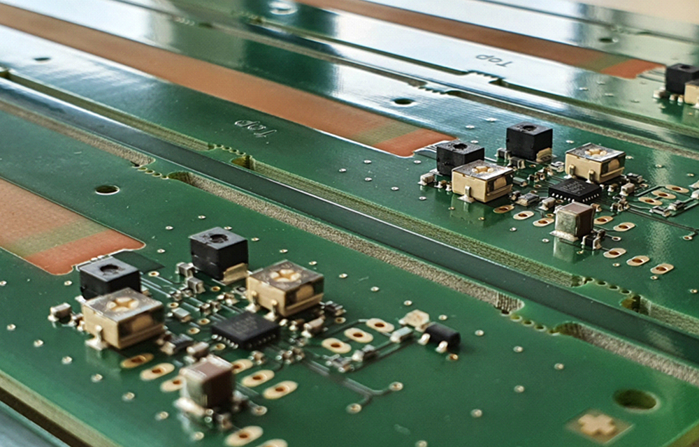
Furthermore, the integration of printed waveguides into printed circuit boards is being researched. Two approaches are being pursued here: the assembly of waveguides on pre-prepared PCBs (see Fig. 3) and the full-surface lamination of waveguides as an additional layer in PCBs.
ficonTEC is investigating the assembly of waveguides by using novel handling tools for flat components. The difficulty here lies in the optical alignment of at least two waveguide ends, which must be placed in relation to the laser and photodiodes. Full-area lamination is designed at the printed circuit board manufacturer Hotoprint. For this purpose, the waveguides must be produced with additional cladding layers to ensure optical functionality. To be able to use lamination, the thermal and mechanical stability as well as the parameters during the process, which the waveguides must survive, are examined.
The laminated waveguides still have to be operated with separately mounted diodes. For this purpose, a concept with separate placement elements from Siemens is being investigated, with which the diodes can couple directly into the waveguides without optical auxiliary elements. The focus here is on the acceptance of the planned solution in industrial production environments.
Potentials and benefits of optical printed circuit boards
The aim of the project is to implement electro-optical printed circuit boards employing optical waveguide integration. These are to be produced cost-effectively and adaptively based on printed optical waveguides. This makes it possible to implement various optical functions that can be used in the future as passive optical networks, optical bus systems, or even optical sensors.
Possible applications are in the high-tech sector in electromobility and communications technology, but also in mass products such as intelligent packaging and lighting applications.
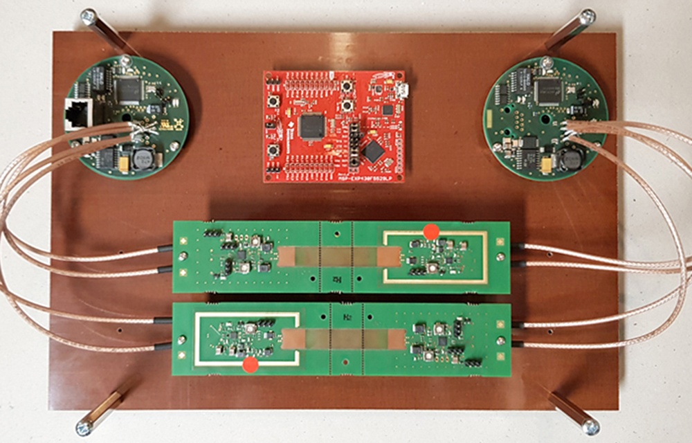
At the project’s mid-term milestone meeting, a first demonstrator could already be shown, which was able to depict the essential function of an optical peer-to-peer network using the printed optical waveguide (see Fig. 4).