Miniaturization of the periphery plays a major role in the miniaturization of quantum systems. Especially in vacuum systems, the pumping technology is the most space-consuming component. As part of the project “Innovative Vacuum Technology for Quantum Sensors” (InnoVaQ), the IMPT is therefore developing a miniaturized pumping technology: an ion getter pump.
Ion getter pump: functional principle
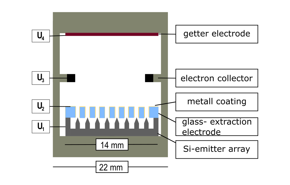
A miniaturized ion getter pump consists of three essential components: an electron source (also called emitter), an electron collector and a getter electrode.
In the electron source, free electrons are generated by field emission. In this process, the electrons leave the solid by tunneling due to a strong electric field. To initiate the field emission, high voltages are needed, often in the high voltage range (kilovolts). These voltages can be minimized by the geometry of the field emitters. By creating tip-like microstructures, the electric field lines bundle in the region of the peaks, which enables tunneling.
The free electrons are pulled toward the electron collector and accelerated in the direction of the getter electrode. Along the way, the free electrons strike the residual gas atoms and ionize them. The resulting positive ions are attracted to the negatively charged getter electrode.
The getter electrode consists of a non-evaporable getter material (NEG). This material ensures that the positive ions are absorbed. Thus, by absorbing the residual gas ions into the getter solid, the number of residual gas atoms is reduced and a prevailing pressure is maintained or minimized, which is the main function of a miniaturized vacuum pump.
Electron source from field emitter arrays
IMPT is currently researching the fabrication of a chip that makes up part of the ion getter pump: the emitter chip. This consists of an electron source and a glass extraction electrode.
The electron source, in the form of arrays of field emitters (FEAs), is typically fabricated by using microtechnology techniques such as reactive ion deep etching, wet chemical etching, or laser ablation, etc..
The field emitters typically have a conical shape. Arrays can even consist of up to 300,000 field emitters, with a single microstructure having a height of about 15 µm and a tip radius in the nanometer range – all in a small space of a few square centimeters.
Cost-efficient production by wafer dicing
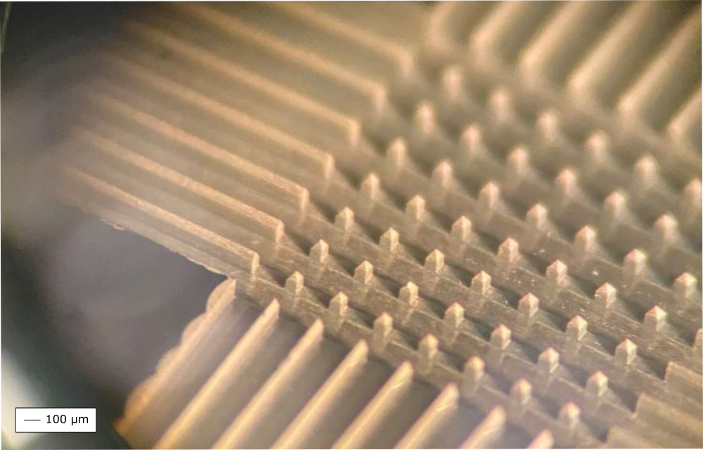
The scientists at IMPT are taking a different approach and manufacturing the electron source from silicon using wafer dicing. Leibniz University Hannover has patented this process. The advantage is the cost efficiency of this manufacturing method, as well as the stability of the field emitters due to their size.
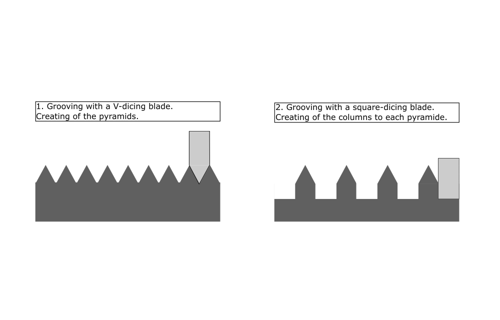
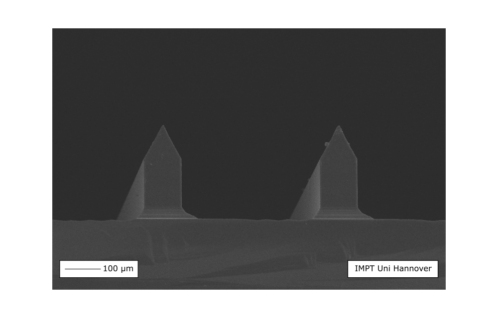
The manufacturing process consists of two steps. In the first step, the pyramid-shaped tips of the emitters are produced with a “V-shaped” dicing blade with a thickness of 200 µm by grooving very close to each other. The wafer is then rotated 90° in the dicing machine and the cut is repeated.
In the second step, a “square” dicing blade is used, which is usually used for dicing chips. This particular blade is used to produce the columns, i.e. the base, for the respective pyramids. This is done by grooving about 250 µm deep into the substrate so that the total height of an emitter is about 250 µm. This step is also repeated after rotation by 90°. The width of the emitters can be adjusted by several overlap cuts or different blade thicknesses.
Useful: The brittleness of silicon
The IMPT produces field emitters with a width of 100 µm. The array size is 12 x 12 emitters on an area of 5 cm². The number of emitters can be scaled up as desired. However, this leads to a higher process time.
Compared to micro-engineered arrays, the number is significantly lower, but an advantage of this method is the use of the brittleness of silicon. This leads to breakouts of the material during the wafer dicing process. Because many breakouts are produced on one emitter, the total number of emission sources is significantly higher and comparable to those produced by using microtechnology techniques. Secondary tips manufactured in this way contribute to field emission and can reduce the necessary high voltage.
With the systems fabricated at IMPT to date and a distance to the extraction electrode of about 600 µm, emission currents of several µA could be measured.
Fabrication of the glass extraction electrode
Glass, as an excellent insulator, is becoming more and more important in microtechnology. The fact that the InnoVaQ extraction electrode is made of glass means that it does not have to be additionally electrically insulated from the electron source. In order to generate a field enhancement in the area of the tips, there is a through-hole in the electrode above each tip. In order to be able to apply a voltage so that an electric field can be generated, the inner walls of this feedthrough must be conformally metallized.
The glass electrode itself is manufactured by LPKF. A laser-induced deep etch technology (LIDE) developed by LPKF is used for production. In this two-step process, the desired areas in the glass are first modified with a laser and then etched with hydrofluoric acid (HF). During the etching process, the etch rate of the modified areas is much higher than that of the non-modified areas. In this process, structures with a high aspect ratio and without the formation of microcracks can be produced.
In the case of the InnoVaQ electrode, the feedthroughs have a diameter of around 100 µm with a glass thickness of 300 – 500 µm. IMPT is currently working on both a suitable metallization process for the electrode and a suitable glass-silicon bonding process for the emitter chip.
Future application
As part of the InnoVaQ project, IMPT and its project partners are developing a vacuum system in which the pressure should be maintained within the ultra-high vacuum (UVH) range between 10-8 and 10-11 mbar. To achieve this pressure, a combination of backing pumps and high vacuum pumps is needed, since single stage pumping from atmospheric pressure to UHV is not possible. The emitter tips fabricated at IMPT act as electron sources for ionization. The miniaturized pump developed should be able to maintain and measure pressure.