Smaller components, smaller tools
The miniaturization of micro-machined components is accompanied by an analogous miniaturization of the tools, which have to meet even higher requirements. This requires innovations in the manufacturing process on the way to downsized and complex tool structures of high quality and comprehensive functionality. Microsystems technology offers a way to manufacture such tools.
Possible application scenarios for the miniaturized tools include the production of microfluidic or biological systems, such as a lab-on-chip in which the polymerase chain reaction (PCR) for the amplification of genetic material can be realized in the smallest installation space. Another aspect is the need for a functional surface, for example to reduce friction and wear or to modify special material properties, which is reflected in an increase in the performance of the component.
One application is a streamlined design of the car body surface in the automotive industry. In this case, the use of micro-milling cutters makes it possible to use them in a mostly conventional machine tool without, for example, requiring a clean room environment, as is the case with comparable processes currently in use.
Thousands of milling cutters in one batch
In microsystems technology, micro-milling cutters enable the production of structures in the sub-millimeter range down to a few micrometers. The reduction in tool diameter comes with challenges, which must be taken into account when designing such tools. On the one hand, this can be a rounding of the cutting edge, and on the other hand, a possible reduction in stiffness can occur.
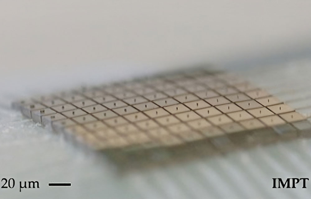
Conventionally available micro-milling cutters are manufactured individually. This means that each individual cutter is eroded from nanocrystalline carbide, which results in high material and time requirements and resulting costs. The batch production approach promises a significant cost reduction for the production of the individual milling cutter despite a comprehensive process chain. The 4-inch substrate used in the development provides the surface area for 5,200 micromilling heads, which can be produced simultaneously.
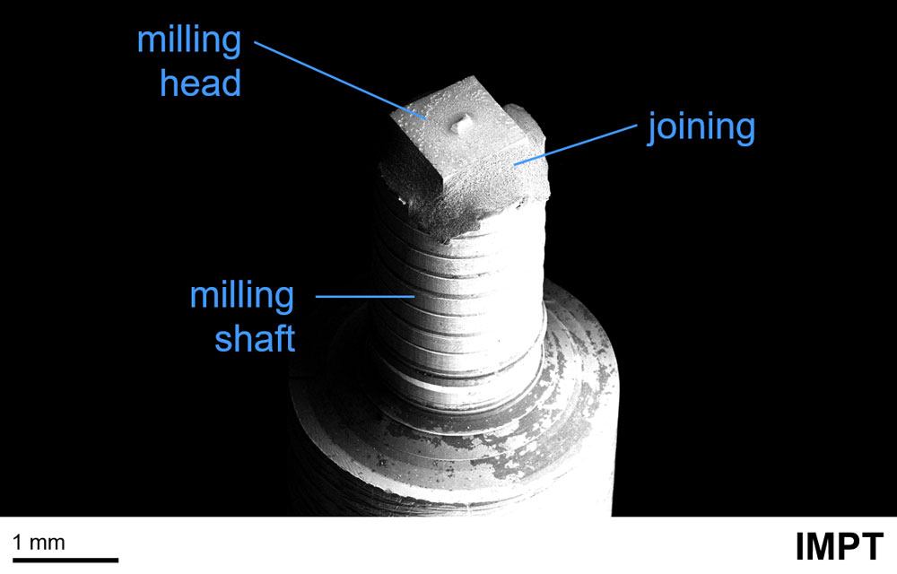
IMPT has been involved in the past with the development of double-edged micro-milling cutters. These consist of a two-part system. A milling head made of silicon carbide (SiC) and a milling shank made of steel. The cutting diameter produced is between 50 and 200 μm and the geometry can be flexibly adapted to the application in the future, for example the material or the required milling contour.
High-performance material silicon carbide
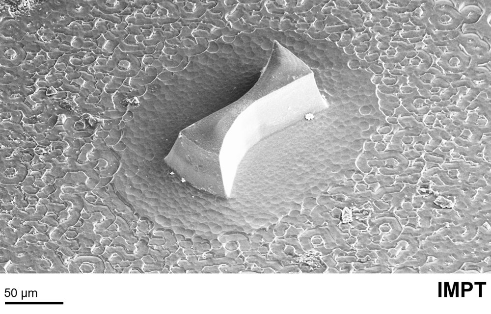
The material used for the milling heads, monocrystalline silicon carbide, brings decisive advantages. In semiconductor technology, silicon carbide has already been used for some time for the production of chips in high-performance electronics, and it can be structured 2.5-dimensionally by means of etching processes. Furthermore, silicon carbide allows photolithographic processing, in which a structure transfer takes place by means of a mask. In this way, the material can be selectively physically and chemically removed by reactive ion etching, thus macroscopically changing the surface topography.
Silicon carbide exhibits special material properties not only in the field of electronics and microsystems technology. The mechanical properties such as hardness or Young’s modulus reach value ranges of diamond or cubic boron nitride. The material SiC is therefore very well suited as a milling material. These properties result in low material wear and long tool life. This enables the machining of steel, for example, where high loads act on the tool.
From the 4-inch substrate to the ready-to-use milling cutter
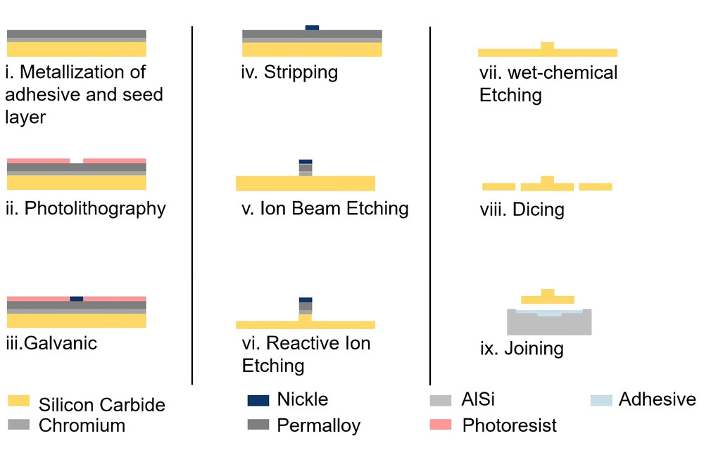
The manufacturing process starts with a 4-inch SiC wafer as substrate. After cleaning, a full-surface metallic nickel coating is applied by sputter deposition to ensure subsequent electrical contacting for an electrodeposition process. Subsequent photolithographic structuring exposes areas where galvanic growth takes place on the exposed metallic surfaces. These areas are critical to the structuring of the cutter geometries later in the process. After the photoresist is removed, ion beam etching is used to remove the metallic coating, leaving the reinforced structures in place.
In a reactive ion etching process, a structure transfer takes place from the generated metallic masking to the SiC substrate. This creates the geometries and cutting edges of the subsequent milling cutters. The metallic mask is then removed by a wet chemical process. In the final back-end processes, the cutters are partition-ground from the 4-inch substrate to a chip width of one millimeter and finally placed on the cutter shank with an epoxy-based UV-curable adhesive.
Validation of the manufactured cutters
In initial milling tests in materials such as copper and steel, the IMPT was able to investigate and confirm the functionality of the micro cutters produced. The tool lives and milling qualities achieved are in the range of conventional micro-milling cutters. This provides a positive outlook for further development.
In the near future, the IMPT will develop a milling center together with an industrial partner, which will enable an optimal interaction of the factors from the production of the milling cutters and the milling cutters themselves. Boundary points of the future development are both the implementation of a pick-and-place process for joining the cutter head and shank within the machine tool and the realization of a defined process gas environment. There is further potential for optimization in the area of the etching process. Among other things, a multi-stage milling cutter is planned in order to be able to remove the chips generated during milling in a more targeted manner and thus reduce wear.